Intel's head of architecture, Raja Koduri.
The processing of neural networks for artificial intelligence is becoming a main part of the workload of every kind of chip, according to chip giant Intel, which on Thursday unveiled details of forthcoming processors during its annual "Architecture Day" ritual.
"Neural nets are the new apps," said Raja M. Koduri, senior vice president and general manager of Intel's Accelerated Computing Systems and Graphics Group, in an interview with ZDNet via Microsoft Teams.
"What we see is that every socket, it's not CPU, GPU, IPU, everything will have matrix acceleration," said Koduri.
Koduri took over Intel's newly formed Accelerated Computing Unit in June as part of a broad re-organizaton of Intel's executive leadership under CEO Pat Gelsinger.
Koduri claimed that by speeding up the matrix multiplications at the heart of neural networks, Intel will have the fastest chips for machine learning and deep learning, and any form of artificial intelligence processing.
Also: Intel forms Accelerated Computing, Software business units
"We are the fastest AI CPU, and our Sapphire Rapids, our new data center architecture, is the fastest for AI workloads," said Koduri.
"Our new GPUs — nobody so far, there have been dozens of startups, but nobody beat Nvidia on a training benchmark, and we have demonstrated that today," he said, alluding to AI chip startups such as Cerebras Systems.
Intel showed a demonstration as part of Architecture Day in which its forthcoming stand-alone GPU, Ponte Vecchio, bested Nvidia's A100 GPU in a common benchmark neural network task, running the ResNet-50 neural network to categorize images from the ImageNet library of photographs.

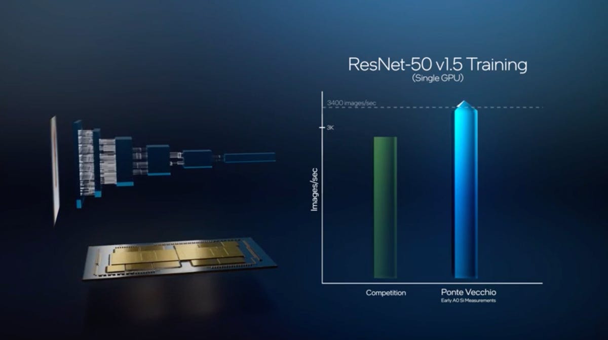
Intel claims pre-prodution versions of its Ponte Vecchio GPU can best Nvidia at a standard measure of neural network performance in deep learning applications, where the ResNet-50 neural network has to be trained to process thousands of images per second from the ImageNet picture collection.

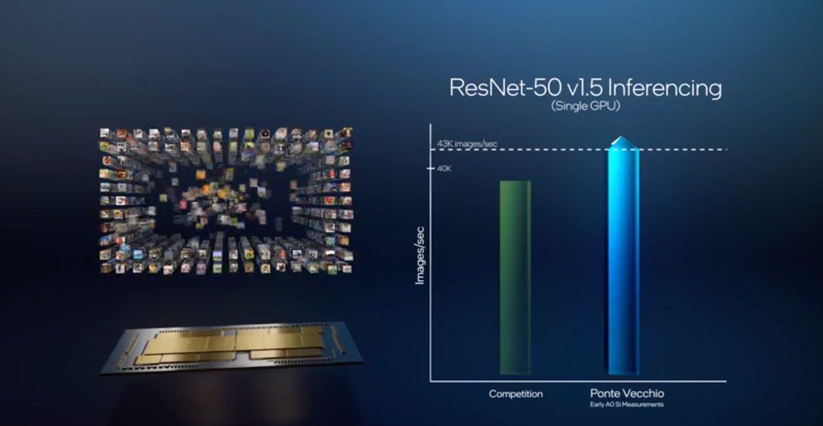
Intel claims Ponte Vecchio can also create predictions faster with ResNet-50 on ImageNet compared to Nvidia and others in what's known as inferene tasks.
In the demonstration, Intel claims Ponte Vecchio, in pre-production silicon, is able to process over 3,400 of the images in one second, topping previous records of 3,000 images. That is for neural network training. In the area of inference, where a trained neural net makes predictions, Ponte Vecchio is able to make predictions for over 43,000 images in a single second, topping what it cites as the existing top score of 40,000 images per second.
Intel's Xeon chips have tended to dominate the market for AI inference, but Nvidia has been making inroads. Intel has litle share in neural network training while Nvidia dominates the field with its GPUs.
Koduri said the company intends to compete against Nvidia in the annual bake-off of AI chips, MLPerf, where Nvidia typically walks away with bragging rights on ResNet-50 and other such benchmark tasks.
The architecture day focuses on Intel's roadmap for how its chips' design of circuits will lay out the transistors and the functional blocks on the chip, such as arithmetic logic units, caches and pipelines.
An architecture change, for Intel or for any company, brings new "cores," the heart of the processor that controls how the "datapath" is managed, meaning, the storage and retrieval of numbers, and the control path, meaning, the movement of instructions around the chip.
Many aspects of the new CPUs have been disclosed previously by Intel, including at last year's Architecture Day. The company has to get software designers thinking about, and working on, its processors years before they are ready to roll off the line.
For instance, the world has known Intel was going to bring to market a new CPU for client computing, called Alder Lake, which combines two kinds of CPUs. On Thursday, Intel announced it would rename those two, formerly code-named Golden Cove and Gracemont, as "Performance Core" and "Efficient Core." More details on that from ZDNet's Chris Duckett.
Also: Intel unveils Alder Lake hybrid architecture with efficient and performance cores
Among the new disclosures today are that the new CPUs will make use of a hardware structure known as the "Thread Director." The Thread Director takes control of how threads of execution are scheduled to be run on the processor in a way that adjusts to factors such as energy use, to relieve the operating system of some of that role.
Thread Director, Intel says in prepared remarks, "provides low-level telemetry on the state of the core and the instruction mix of the thread, empowering the operating system to place the right thread on the right core at the right time."
"The entire way the OS interacts with hardware is a hardware innovation," observed Koduri in the ZDNet interview.

Thread Director, a hardware schedular that will take over some responsibilty for managing threads of instruction from the operating system, was one of the new items discussed at Intel's archticture day.
IntelAnother new disclosure is how the chips will make use of memory bandwidth technologies. For example, Alder Lake will support PCIe Gen 5, DDR 5 memory interfaces, it was disclosed. Intel's forthcoming data center processor, Sapphire Rapids, includes ways to spread data across both DDR 5 main memory and high-bandwidth HBM memory without the application software having to know anything about either chips. That allows for both memory capacity and memory bandwidth to increase steadily, for AI workloads that demand both aspects of memory and I/O.
Intel disclosed for the first time certain performance metrics for Sapphire Rapids, which constitutes the next era of its Xeon family of server chips. For example, the chip will perform 2,048 operations per clock cycle on 8-bit integer data types using what Intel calls its AMX, or "advanced matrix extensions." Again, the emphasis is on neural net kinds of operations. AMX is a special kind of matrix multiplication capability that will operate across separate tiles of a chip. Sapphire Rapids is composed of four separate physical tiles that each have CPU and accelerator and input/output functions, but that look to the operating system like one logical CPU.

Intel claims Sapphire Rapids is optimized for AI via extensions such as AMX.
IntelSapphire Rapids is an example of how Intel is increasingly looking to the physical construction of chips across multiple substrates as an advantage. The use of multiple physical tiles, for example, rather than one monolithic semiconductor die, makes use of what Intel dubs its embedded multi-die interconnect bridge.
Thursday's presentation featured lots of discussion of Intel process technology as well, which the company has been seeking to straighten out after mis-steps in recent years.
Because of the limits of Moore's Law's traditional scaling of transistor size, said Koduri, it is essential to utilize other advantages that Intel can bring to chip making, including stacking of multiple die within a package.
"Today it is far more important for architects to leverage every tool in our process and packaging tool chest than it was a decade ago to build this stuff," said Koduri. "Before, it was, yeah, yeah, yeah, the traditional Dennard Scaling, Moore's Law took care of it, take my new CPU, put it on the new process node, you get it done."

He was referring to the observation by Robert Dennard, a scientist at IBM, in the 1970s that as more and more transistors are packed into a square area of a chip, the power consumption of each transistor goes down so that the processor becomes more power-efficient. Dennard Scaling is regarded as being effectively dead, just like Moore's Law.
Both Alder Lake and Sapphire Rapids will be built by Intel using what it is calling its "Intel 7" process technology. That is a renaming of what had been called "10nm Enhanced SuperFin," whereby the company adds a more-efficient three-dimensional transistor, a FinFet, to the 10-nanometer process for greater efficiency of energy usage. (The Intel 7 designation is part of a broad renaming of Intel's process technology that the company unveiled in July.)
At the same time, some of Intel's parts will be made using production at Taiwan Semiconductor Manufacturing, which supplies Intel's competitors. That move to outsource selectively is an extension of Intel's existing use of outsourced transistor production. It is what CEO Gelsinger has called Intel's "IDM 2.0" strategy.
Also: Intel: Data bandwidth, sparsity are the two biggest challenges for AI chips
Today, said Koduri, "it is a golden age for architects because we have to use these tools much more effectively." Koduri was echoing a claim made in 2019 by U.C. Berkeley professor David Patterson that computer architects have to compensate for the device physics that mean Moore's Law and Dennard Scaling no longer dominate.
Of course, with Nvidia continuing to innovate in GPUs, and now planning to build its own CPU, "Grace," in coming years, and with startups such as Cerebras Systems building entirely new kinds of chips for AI, the target for Intel in AI is not simply to make its processors more AI-friendly. Rather, the goal must be to change the way the field of AI goes about its work.
Asked how Intel's various innovations may change the way neural networks are built, Koduri said that the numerous kinds of processor types now proliferating at Intel and elsewhere will have to cooperate much more and function less apart, to share tasks.
"The workloads are definitely going in the direction where these things called CPUs, GPUs, DPUs, and memories talk to each another way more than they are talking to each other right now."
"They will be talking to each other, they'll be in closer collaboration between these things, to get the work done, than you have seen in the first five years of deep learning."
Koduri was referring to the period of 2016 to 2021 as "the first five years of deep learning," as he sees it. "The next five years will bring all these things closer together."
Intel architect Koduri says every chip will be a neural net processor - ZDNet
Read More

No comments:
Post a Comment